5 Configuration space decoding
PCI defines a third address space in addition to memory and I/O. This is called configuration space and every logical functiongets 256 bytes in this space. A function is selected for configuration space access by asserting the corresponding device’s IDSEL signal together with executing a Configuration Read or Configuration Write bus command.
Configuration Transactions
PCI-based systems require a mechanism that allows software to generate transactions to Configuration space. This mechanism will generally be located in the Host-to-PCI bridge. The specification defines an appropriate mechanism for x86 processors. The x86 configuration mechanism uses two DWORD read/write registers in I/O space. These are:
CONFIG_ADDRESS 0x3f8
CONFIG_DATA 0x3fc
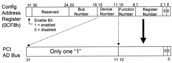
The layout of CONFIG_ADDRESS is shown in Figure 9. Bit 31 is an enable that determines when access to CONFIG_DATA is to be interpreted as a configuration transaction on the PCI bus. When bit 31 is 1, reads and writes to CONFIG_DATA are translated to PCI configuration read and write cycles at the address specified by the contents of CONFIG_ADDRESS. When bit 31 is 0, reads and writes to CONFIG_DATA is simply passed through as PCI I/O reads and writes. Bits 30 to 24 are reserved, read-only, and must return 0 when read. Bits 23 to 16 identify a specific bus segment in the system. Bits 15 to 11 select a device on that segment. Bits 10 to 8 select a function within the device (if the device supports multiple functions). Bits 7 to 2 select a DWORD configuration register within the function. Finally, bits 1 and 0 are reserved, read-only, and must return 0 when read.
CONFIG_ADDRESS can only be accessed as a DWORD. Byte or word accesses to CONFIG_ADDRESS are passed through to the PCI bus.

Configuration Header — Type 0
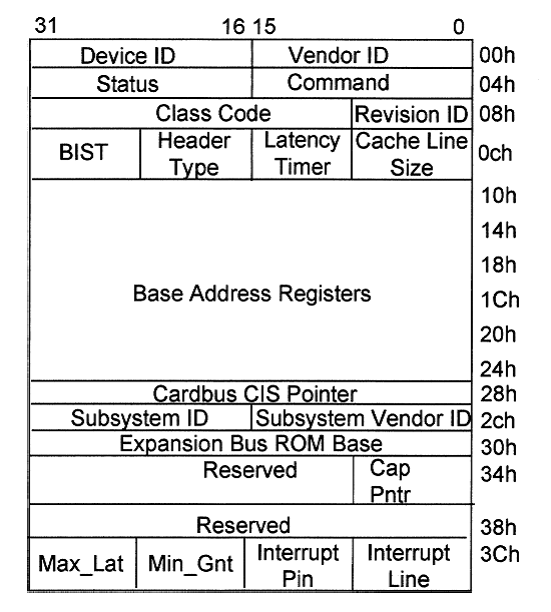
Of the 256 bytes of configuration space allocated to every function, the first 64 bytes are defined by the specification and are called the Configuration Header. The remaining 192 bytes are available for device-specific configuration functions. Figure 10 shows the layout of the Configuration Header.
Header Type
Currently, three different header types are defined as indicated by the value in byte 0xE (14 decimal). The Type 0 header is for most devices. The Type 1 header describes a bridge device and the Type 2 header describes a PC Card device. In all cases, the first three DWORDS and the Header Type byte of the fourth DWORD are the same. The most significant bit of the Header Type is set to 1 if the device is a multi-function device.
Identification Registers
Several fields in the header are read-only and serve to identify the device along with various operational characteristics.

Vendor ID:Identifies the vendor of the device. More specifically, it identifies the vendor of the PCI silicon. Vendor ID codes are assigned by the PCI SIG.
Device ID:Identifies the device. This value is assigned by the vendor.
Revision ID: Assigned by the device vendor to identify the revision level of the device.
Two additional registers allow makers of PCI plug in adapters to identify their devices.
Subsystem Vendor ID:Identifies the vendor of a functional PCI device.
Subsystem Device ID:Assigned by the vendor to identify a functional PCI
device, can also be used to identify individual functions in a multi-function device.
The Class Code is a 24-bit read-only register that identifies the basic function of the device. It is divided into three sections:
Base Class:Defines the basic functional category.
Sub-class:Identifies a device type or implementation within the Base Class. For example, a mass storage controller can be SCSI, IDE, floppy, etc. A network controller can be Ethernet, token ring and so on.
Programming Interface:Defines specific register-level implementations. For most classes this is simply 0, but it is used for IDE controllers and other traditional PC peripherals.
Command Register: The read/writable Command Register provides coarse control over a device’s ability to generate and respond to PCI cycles.
Status Register: The Status Register contains two types of information — Read only bits that convey additional information about a device’s capabilities and read/write bits that track bus related events.
Base Address Registers (BAR): The Base Address Registers provide the mechanism that allows configuration software to determine the memory and I/O resources that a device requires. Once the system topology is determined, configuration software maps all devices into a set of reasonable, non-conflicting address ranges and writes the corresponding starting addresses into the Base Address Registers. The Type 0 configuration header supports up to six Base Address Registers, allowing a device to have up to six independent address ranges.
Chapters:
- Introduction to PCI protocol
- PCI Signal Descriptions
- PCI Bus Transactions
- PCI Bus Timing Diagrams
- Configuration space decoding
- Arbitration process under PCI
- Error Detection and Reporting
Bibliography
- PCI Tutorial by Xilinx
- PCI Bus Demystified by Doug Abbott
Submitted by: Rovin and Sagar

i cannot access anything but the first page
Hi,
Nice post, but you may want to fix Chapter 5: Configuration space decoding.
“CONFIG_ADDRESS 0x3f8
CONFIG_DATA 0x3fc”
0x3F8 and 0x3FC are UART0, not the PCI registers. Note that the diagram shows the correct address.
I understand PCI finally….Thanks….
I would know the différence between the PCI prtocol and VME protocol.
if it is possible! thanks
Historians have found references to early forms of baseball from the 1820’s and 1830’s in New York City state, Philadelphia,
Massachusetts, New Hampshire, Vermont, and other northeastern states.
8 years ago, Jung Da-Yeon was a homely, out-of-shape Korean woman. 19
But Mary kept all these things and pondered them in her heart.