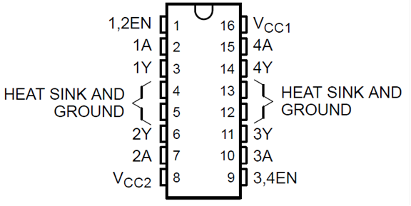
PIN CONFIGURATION:
Here is the pin configuration.
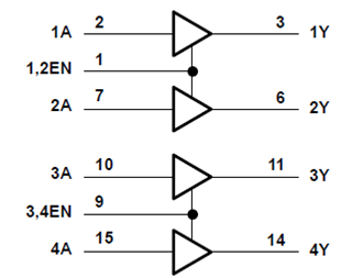
LOGIC DIAGRAM:
DESCRIPTION/ORDERING INFORMATION:
The L293 and L293D are quadruple high-current half-H drivers. The L293 is designed to provide bidirectional drive currents of up to 1 A at voltages from 4.5 V to 36 V. The L293D is designed to provide bidirectional drive currents of up to 600-mA at voltages from 4.5 V to 36 V. Both devices are designed to drive inductive loads such as relays, solenoids, dc and bipolar stepping motors, as well as other high-current/high-voltage loads in positive-supply applications. All inputs are TTL compatible. Each output is a complete totem-pole drive circuit, with a Darlington transistor sink and a pseudo- Darlington source. Drivers are enabled in pairs, with drivers 1 and 2 enabled by 1,2EN and drivers 3 and 4 enabled by 3,4EN.
When an enable input is high, the associated drivers are enabled, and their outputs are active and in phase with their inputs. When the enable input is low, those drivers are disabled, and their outputs are off and in the high-impedance state. With the proper data inputs, each pair of drivers forms a full-H (or bridge) reversible drive suitable for solenoid or motor applications. On the L293, external high-speed output clamp diodes should be used for inductive transient suppression. A VCC1 terminal, separate from VCC2, is provided for the logic inputs to minimize device power dissipation. The L293and L293D are characterized for operation from 0°C to 70°C.
TRANSISTOR AS A SWITCH:
The transistor is the fundamental building block of modern electronic devices, and its presence is ubiquitous in modern electronic systems.
Because a transistor’s collector current is proportionally limited by its base current, it can be used as a sort of current-controlled switch. A relatively small flow of electrons sent through the base of the transistor has the ability to exert control over a much larger flow of electrons through the collector.
When used as an AC signal amplifier, the transistors Base biasing voltage is applied so that it operates within its “Active” region and the linear part of the output characteristics curves are used. However, both the NPN & PNP type bipolar transistors can be made to operate as an “ON/OFF” type solid state switch for controlling high power devices such as motors, solenoids or lamps. If the circuit uses the Transistor as a Switch, then the biasing is arranged to operate in the output characteristics curves seen previously in the areas known as the “Saturation” and “Cut-off” regions as shown below.
TRANSISTOR CURVES:
![]()
The shaded area at the bottom represents the “Cut-off” region. Here the operating conditions of the transistor are zero input base current (Ib), zero output collector current (Ic) and maximum collector voltage (Vce) which results in a large depletion layer and no current flows through the device. The transistor is switched “Fully-OFF”. The lighter blue area to the left represents the “Saturation” region. Here the transistor will be biased so that the maximum amount of base current is applied, resulting in maximum collector current flow and minimum collector emitter voltage which results in the depletion layer being as small as possible and maximum current flows through the device. The transistor is switched “Fully-ON”. Then we can summarize this as:
Ø Cut-off Region: Both junctions are Reverse-biased, Base current is zero or very small resulting in zero Collector current flowing, the device is switched fully “OFF”.
Ø Saturation Region: Both junctions are Forward-biased, Base current is high enough to give a Collector-Emitter voltage of 0v resulting in maximum Collector current flowing, the device is switched fully “ON”.
TRANSISTOR SWITCHING CIRCUIT:
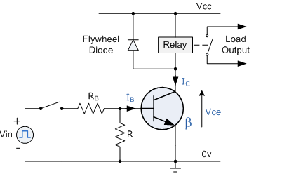
An NPN Transistor as a switch being used to operate a relay is given above. With inductive loads such as relays or solenoids a flywheel diode is placed across the load to dissipate the back EMF generated by the inductive load when the transistor switches “OFF” and so protect the transistor from damage. If the load is of a very high current or voltage nature, such as motors, heaters etc, then the load current can be controlled via a suitable relay as shown.
The circuit resembles that of the Common Emitter circuit we looked at in the previous tutorials. The difference this time is that to operate the transistor as a switch the transistor needs to be turned either fully “OFF” (Cut-off) or fully “ON” (Saturated). An ideal transistor switch would have an infinite resistance when turned “OFF” resulting in zero current flow and zero resistance when turned “ON”, resulting in maximum current flow. In practice when turned “OFF”, small leakage currents flow through the transistor and when fully “ON” the device has a low resistance value causing a small saturation voltage (Vce) across it. In both the Cut-off and Saturation regions the power dissipated by the transistor is at its minimum.
To make the Base current flow, the Base input terminal must be made more positive than the Emitter by increasing it above the 0.7 volts needed for a silicon device. By varying the Base-Emitter voltage Vbe, the Base current is altered and which in turn controls the amount of Collector current flowing through the transistor as previously discussed. When maximum Collector current flows the transistor is said to be saturated. The value of the Base resistor determines how much input voltage is required and corresponding Base current to switch the transistor fully “ON”.
Transistor switches are used for a wide variety of applications such as interfacing large current or high voltage devices like motors, relays or lamps to low voltage digital logic IC’s or gates like AND Gates or OR Gates.
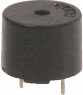
BUZZER:
Sound is simply a wave of varying air pressure. These pressure waves cause a thin membrane in the ear to vibrate and the brain interprets these vibrations as sound. A decibel (dB) scale is used to describe the sound pressure level (SPL) or loudness of a sound.
In general, man’s audible frequency range is about 20 Hz to 20 kHz. Frequency ranges of 2 kHz to 4 kHz are most easily heard. For this reason, most piezoelectric sound components are used in this frequency range, and the resonant frequency (f0) is generally selected in the same range too.
Piezoelectric sound components are used in many ways such as home appliances, OA equipment, audio equipment telephones, etc. And they are applied widely, for example, in alarms, speakers, telephone ringers, receivers, transmitters, beep sounds, etc.
ISP PROGRAMMER:
In-System Programming (abbreviated ISP) is the ability of some programmable logic devices, microcontrollers, and other programmable electronic chips to be programmed while installed in a complete system, rather than requiring the chip to be programmed prior to installing it into the system. Otherwise, In-system programming means that the program and/or data memory can be modified without disassembling the embedded system to physically replace memory.
The primary advantage of this feature is that it allows manufacturers of electronic devices to integrate programming and testing into a single production phase, rather than requiring a separate programming stage prior to assembling the system. This may allow manufacturers to program the chips in their own system’s production line instead of buying preprogrammed chips from a manufacturer or distributor, making it feasible to apply code or design changes in the middle of a production run.
ISP (In System Programming) will provide a simple and affordable home made solution to program and debug your microcontroller based project.
Normally, the flash memory of an ATMEL microcontroller is programmed using a parallel interface, which consists of sending the data byte by byte (using 8 independent lines for the data, and another bunch of lines for the address, the control word and clock input).
Many members of the Maxim 8051-based microcontroller family support in-system programming via a commonly available RS-232 serial interface. The serial interface consists of pins SCK, MOSI (input) and MISO (output) and the RST pin, which is normally used to reset the device.
ISP is performed using only 4 lines, and literally, data is transferred through 2 lines only, as in a I2C interface, where data is shifted in bit by bit though MOSI line, with a clock cycle between each bit and the next (on the SCK line). MISO line is used for reading and for code verification; it is only used to output the code from the FLASH memory of the microcontroller.
The RST pin is also used to enable the 3 pins (MOSI, MISO and SCK) to be used for ISP simply by setting RST to HIGH (5V), otherwise if RST is low (0V), program start running and those three pins, are used normally as P1.5, P1.6 and P1.7. After RST is set high, the Programming Enable instruction needs to be executed first before other operations can be executed. Before a reprogramming sequence can occur, a Chip Erase operation is required. The Chip Erase operation turns the content of every memory location in the Code array into FFH.
Either an external system clock can be supplied at pin XTAL1 or a crystal needs to be connected across pins XTAL1 and XTAL2. The maximum serial clock (SCK) frequency should be less than 1/16 of the crystal frequency. With a 33 MHz oscillator clock, the maximum SCK frequency is 2 MHz.
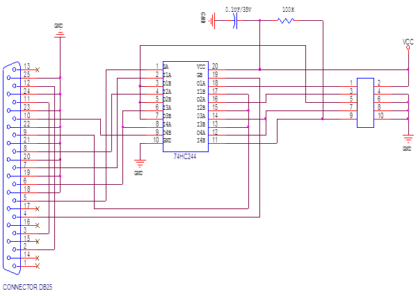
In the above figure we can see the ISP programmer connections using 74ls244
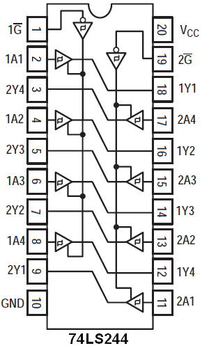
74LS244:
The 74LS244 is used to work between PRINT ports to the chips AT89S52. We cannot observe 74LS244 on the PCB which is AT89S52 located. It hid in the joint between PC and 6 transmission lines. The 74LS244 pin configuration, logic diagram, connection and function table is on the below.
ATMEL ISP FLASH PROGRAMMER:
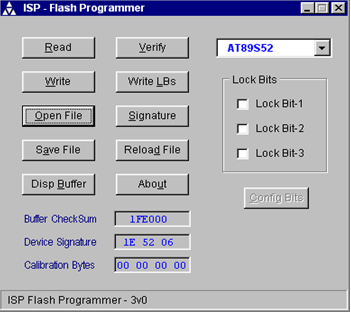
This is the software that will take the HEX file generated by whatever compiler you are using, and send it – with respect to the very specific ISP transfer protocol – to the microcontroller.
This programmer was designed in view of to be flexible, economical and easy to built, the programmer hardware uses the standard TTL series parts and no special components are used. The programmer is interfaced with the PC parallel port and there is no special requirement for the PC parallel port, so the older computers can also be used with this programmer.
SUPPORTED DEVICES:
The programmer software presently supports the following devices
AT89C51 AT89S51 AT89C1051 UD87C51 AT89C52 AT89S52 AT89C2051 D87C52 AT89C55 AT89S53 AT89C4051 AT89C55WD AT89S8252 AT89C51RC
Note: For 20 pin devices a simple interface adapter is required.
The ISP-3v0.zip file contains the main program and the I/O port driver for
Windows 2000 & XP. Place all files in the same folder, for win-95/98 use the “ISP-Pgm3v0.exe”File, for win-2000 & XP use the “ISP-XP.bat” file. The main screen view of the program is shown in fig below.
your project is cool but mine is better..
…….
Sir can send me the codes used in this project? rjaylui@yahoo.com! Thanks a lot!
Sir can you send me the codes used in this project? rjaylui@yahoo.com! Thanks a lot!
The source code shows error when compiling pls help
pls send me the code
uthmanjta@gmail.com
the source code contains somany error. dont waste ur time in this project. i request the author pls post the correct code and hex.
but no answer from the autor and admin?????????????????????????????????????????/
send me this code sir……
SIR I READ THIS PROJECT ITS NICE …… PLEASE, CAN U SEND SOURCE CODE TO MY MAILID rk_yadav1@yahoo.com
i need the god damn code of pc operation control using ir remote
If u want embedded project pls contact me. (with report&program). Unaiskavot1@gmail.com