FEATURES:
- Photo detector and preamplifier in one package
- Internal filter for PCM frequency
- Improved shielding against electrical field disturbance
- TTL and CMOS compatibility
- Output active low
- Low power consumption
- High immunity against ambient light
- Continuous data transmission possible (up to 2400 bps)
- Suitable burst length ?10 cycles/burst
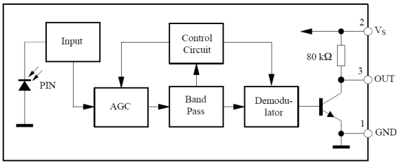
BLOCK DIAGRAM:
APPLICATION CIRCUIT:
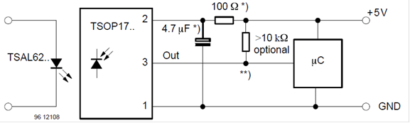
This is recommended to suppress power supply disturbances. The output voltage should not be hold continuously at a voltage below 3.3V by the external circuit.
SUITABLE DATA FORMAT:
The circuit of the TSOP1738 is designed in that way that unexpected output pulses due to noise or disturbance signals are avoided. A band pass filter, an integrator stage and an automatic gain control are used to suppress such disturbances. The distinguishing mark between data signal and disturbance signal are carrier frequency, burst length and duty cycle. The data signal should full fill the following condition:
Ø Carrier frequency should be close to center frequency of the band pass (e.g. 38 kHz).
Ø Burst length should be 10cycles/burst or longer.
Ø After each burst which is between 10 cycles and 70 cycles a gap time of at least 14 cycles is necessary.
Ø For each burst which is longer than 1.8ms a corresponding gap time is necessary at some time in the data stream. This gap time should have at least same length as the burst.
Ø DC light (e.g. from tungsten bulb or sunlight)
Ø Continuous signal at 38 kHz or at any other frequency
Ø Signals from fluorescent lamps with electronic ballast
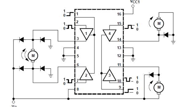
L293D:
Ø 600ma output current capability per channel
Ø 1.2a peak output current (non repetitive) per channel
Ø Enable facility
Ø Over temperature protection
Ø Logical “0” input voltage up to 1.5 v (high noise immunity)
Ø Internal clamp diodes
Ø Wide Supply-Voltage Range: 4.5 V to 36 V
Ø Separate Input-Logic Supply
Ø Internal ESD Protection
Ø Thermal Shutdown
Ø High-Noise-Immunity Inputs
Ø Functionally Similar to SGS L293 and SGS L293D
Ø Output Current 1 A Per Channel (600 mA for L293D)
Ø Peak Output Current 2 A Per Channel (1.2 A for L293D)
Ø Output Clamp Diodes for Inductive Transient Suppression (L293D)
DESCRIPTION:
The Device is a monolithic integrated high voltage, high current four channel driver designed to accept standard DTL or TTL logic levels and drive inductive loads (such as relays solenoids, DC and stepping motors) and switching power transistors. To simplify use as two bridges each pair of channels is equipped with an enable input. A separate supply input is provided for the logic, allowing operation at a lower voltage and internal clamp diodes are included. This device is suitable for use in switching applications at frequencies up to 5 kHz. The L293D is assembled in a 16 lead plastic package which has 4 center pins connected together and used for heat sinking.
BLOCK DIAGRAM:
your project is cool but mine is better..
…….
Sir can send me the codes used in this project? rjaylui@yahoo.com! Thanks a lot!
Sir can you send me the codes used in this project? rjaylui@yahoo.com! Thanks a lot!
The source code shows error when compiling pls help
pls send me the code
uthmanjta@gmail.com
the source code contains somany error. dont waste ur time in this project. i request the author pls post the correct code and hex.
but no answer from the autor and admin?????????????????????????????????????????/
send me this code sir……
SIR I READ THIS PROJECT ITS NICE …… PLEASE, CAN U SEND SOURCE CODE TO MY MAILID rk_yadav1@yahoo.com
i need the god damn code of pc operation control using ir remote
If u want embedded project pls contact me. (with report&program). Unaiskavot1@gmail.com