APPLICATIONS:
- Select Project – Rebuild all target files or Build target.
DEBUGGING AN APPLICATION IN UVISION2:
To debug an application created using uVision2, you must:
- Select Debug – Start/Stop Debug Session.
- Use the Step toolbar buttons to single-step through your program. You may enter G, main in the Output Window to execute to the main C function.
- Open the Serial Window using the Serial #1 button on the toolbar.
- Debug your program using standard options like Step, Go, Break, and so on.
LIMITATIONS OF EVALUATION SOFTWARE:
The following limitations apply to the evaluation versions of the C51, C251, or C166 tool chains. C51 Evaluation Software Limitations:
- The compiler, assembler, linker, and debugger are limited to 2 Kbytes of object code but source Code may be any size. Programs that generate more than 2 Kbytes of object code will not compile, assemble, or link the startup code generated includes LJMP’s and cannot be used in single-chip devices supporting Less than 2 Kbytes of program space like the Philips 750/751/752.
- The debugger supports files that are 2 Kbytes and smaller.
- Programs begin at offset 0x0800 and cannot be programmed into single-chip devices.
- No hardware support is available for multiple DPTR registers.
- No support is available for user libraries or floating-point arithmetic.
EVALUATION SOFTWARE:
- Code-Banking Linker/Locator
- Library Manager.
- RTX-51 Tiny Real-Time Operating System
PERIPHERAL SIMULATION:
The u vision2 debugger provides complete simulation for the CPU and on chip peripherals of most embedded devices. To discover which peripherals of a device are supported, in u vision2. Select the Simulated Peripherals item from the Help menu. You may also use the web-based device database. We are constantly adding new devices and simulation support for on-chip peripherals so be sure to check Device Database often.
AT89S52:
FEATURES:
- Compatible with MCS®-51 Products
- 8K Bytes of In-System Programmable (ISP) Flash Memory
-Endurance: 1000 Write/Erase Cycles
- 4.0V to 5.5V Operating Range
- Fully Static Operation: 0 Hz to 33 MHz
- Three-level Program Memory Lock
- 256 x 8-bit Internal RAM
- 32 Programmable I/O Lines
- Three 16-bit Timer/Counters
- Eight Interrupt Sources
- Full Duplex UART Serial Channel
DESCRIPTION:
The AT89S52 is a low-power, high-performance CMOS 8-bit microcontroller with 8K bytes of in-system programmable Flash memory. The device is manufactured using Atmel’s high-density nonvolatile memory technology and is compatible with the industry-standard 80C51 instruction set and pinout. The on-chip Flash allows the program memory to be reprogrammed in-system or by a conventional nonvolatile memory programmer. By combining a versatile 8-bit CPU with in-system programmable Flash on a monolithic chip, the Atmel 89S52 is a powerful microcontroller which provides a highly-flexible and cost-effective solution to many embedded control applications.
The AT89S52 provides the following standard features: 8K bytes of Flash, 256 bytes of RAM, 32 I/O lines, Watchdog timer, two data pointers, three 16-bit timer/counters, a six-vector two-level interrupt architecture, a full duplex serial port, on-chip oscillator, and clock circuitry. In addition, the AT89S52 is designed with static logic for operation down to zero frequency and supports two software selectable power saving modes. The Idle Mode stops the CPU while allowing the RAM, timer/counters, serial port, and interrupt system to continue functioning. The Power-down mode saves the RAM contents but freezes the oscillator, disabling all other chip functions until the next interrupt or hardware reset.
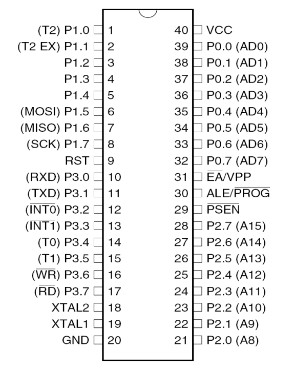
PIN CONFIGURATION 40-lead PDIP:
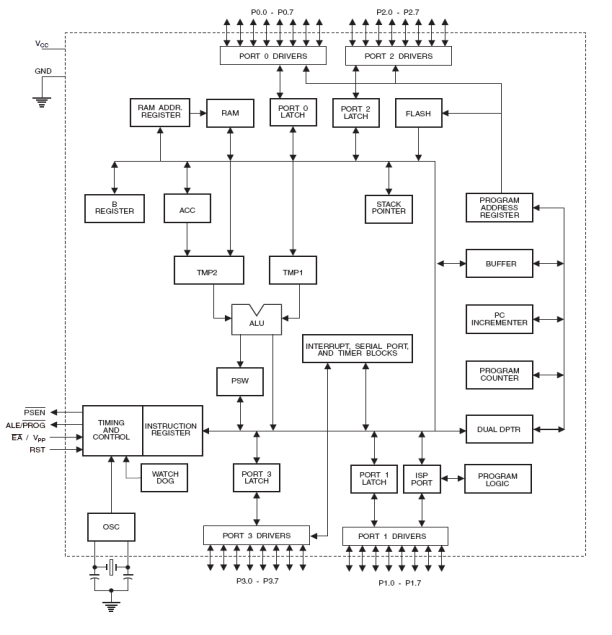
ARCHITECTURE:
PIN DESCRIPTION:
VCC: Supply voltage.
GND: Ground.
Port 0:
Port 0 is an 8-bit open drain bidirectional I/O port. As an output port, each pin can sink eight TTL inputs. When 1s are written to port 0 pins, the pins can be used as high-impedance inputs.
Port 0 can also be configured to be the multiplexed low-order address/data bus during accesses to external program and data memory. In this mode, P0 has internal pull-ups.
Port 0 also receives the code bytes during Flash programming and outputs the code bytes during program verification. External pull-ups are required during program verification.
your project is cool but mine is better..
…….
Sir can send me the codes used in this project? rjaylui@yahoo.com! Thanks a lot!
Sir can you send me the codes used in this project? rjaylui@yahoo.com! Thanks a lot!
The source code shows error when compiling pls help
pls send me the code
uthmanjta@gmail.com
the source code contains somany error. dont waste ur time in this project. i request the author pls post the correct code and hex.
but no answer from the autor and admin?????????????????????????????????????????/
send me this code sir……
SIR I READ THIS PROJECT ITS NICE …… PLEASE, CAN U SEND SOURCE CODE TO MY MAILID rk_yadav1@yahoo.com
i need the god damn code of pc operation control using ir remote
If u want embedded project pls contact me. (with report&program). Unaiskavot1@gmail.com