Experimental Procedure:
The experiment consists of two parts.
PART A: DPSK Modulation.
PART B: DPSK Demodulation.
PART A: DPSK Modulation
1. The DPSK modulator circuit is rigged as shown in the figure. The Y and W, the output of Digital Signal Generator are connected to the analog switches. Hence carrier frequency is adjusted in such a way that in one pulse we should get one and half cycle of carrier signal. The pulse width of the modulating signal is 80ms which refers to 12.5KHz. To get one and half cycle of carrier signal, carrier frequencies set slightly above 18.7KHz.
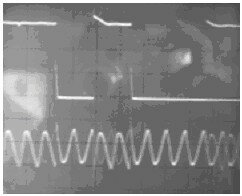
2. The output of the circuit is monitored on the CRO channel. The carrier frequency is slightly adjusted so that during high state of the modulating signal, modulated signal appears like letter M and during low state of the modulating signal, it appears like letter W. The output observed is shown in the figure below with respect to the modulating signal. The waveform observed is coincided with the pulse waveform indicating the perfect ness in the modulation process and no distortion is observed.

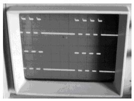
3. Trial is repeated by varying the waveform by adjusting SET PULSE coincided with pulse waveform to see the perfect ness of the modulation. The waveform obtained for 11010011, is shown in the Figure above. The DC input is varied by adjusting SET PULSE knob of ADC.
Part B: DPSK Demodulation
1. DPSK demodulator circuit is rigged as shown in figure using PLL 565. The output from DPSK modulator circuit is connected to DPSK input terminal.
2. The output of the demodulator is observed on CRO channel 2 in comparison with the modulating signal W or Y .
3. The demodulated signal is observed on CRO is finely tuned in the oscillator to get a perfect demodulated signal as shown in the figure below.

A Inverting amplifier and schmitt trigger is used to get proper demodulated output without which there may be slight distortion.
Determination of Bias Distortion:
Modulating signal Y and W are now placed by 0101 sequence. The modulating and demodulated signal observed on CRO as shown in the figure above. From the CRO waveform following time period is noted.
TIRX = 100ms
TITX = 80ms
TORX = 80ms
TOTX = 80ms
Bias distortion is given by
0.5 TIRX
Bd = ——————
TITX +TORX
0.5x100ms
= ——————-
80ms+80ms
= 0.31
= 31%
Determination of Jitter:
From waveform in figure above, the following time period are noted
Tmax = 15ms
Tmin =10ms
Tb = 80ms
Jitter J is given by
Tmax-Tmin
J = —————–
Tb
15ms-10ms
= —————–
80ms
= 0.065
= 6.5%
Result:
DPSK modulation is obtained using analog switch and DPSK demodulation is obtained using PLL IC 565. The modulated and demodulated waveforms are recorded. From the CRO waveform bias distortion and jitter are calculated.
Bd = 31.2%
J = 6.5%

hi…..what signals are given under the name W and Y???
dats a li’l confusing…
pls clarify my doubt soon..
i want information about depsk can u plz tel me about in detailed????
Truly wonderful desgin of this web page. It really is individual and compares for your posts. Don´t give up and make your individual issue!
what r flead and flag signals
why r FET’s used??..
can u plz give the detailed information of how the transmission takes place
pls send a detailed waveforms consisting of delays
i c’t understand the mean of y,w.
furla bags outlet
I have few blogs and very sporadically run out from to post .
Hi your web-site url: http://studentprojects.in/articles/electronics/analog/dpsk-modulation-and-demodulation/ seems to be
redirecting to a completely different web page when I click the home page button. You might want to
have this looked at.
What’s up, just wanted to mention, I loved this post.
It was helpful. Keep on posting!
There’s certainly a lot to find out about this issue.
I like all of the points you’ve made.