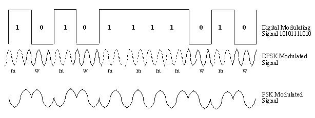
Differential phase shift keying (DPSK), a common form of phase modulation conveys data by changing the phase of carrier wave. In Phase shift keying, High state contains only one cycle but DPSK contains one and half cycle. Figure illustrates PSK and DPSK Modulated signal by 10101110 pulse sequence

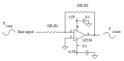
High state is represented by a M in modulated signal and low state is represented by a wave which appears like W in modulated signal DPSK encodes two distinct signals of same frequency with 180 degree phase difference between the two. This experiment requires two 180 degree out of phase carrier and modulating signals. Sine wave from oscillator is selected as carrier signal. DSG converts DC input voltage into pulse trains. These pulse trains are taken as modulating signals. In actual practice modulating signal is digital form of voice or data. Sine wave is selected as carrier and 180 degree phase shift is obtained using Opamp as shown in figure below. Different methods are used to demodulate DPSK. The analog scheme is the PLL (Phase Locked loop).

DPSK Modulation:
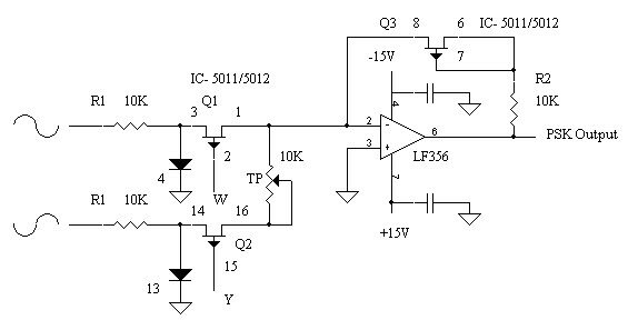
In DPSK, during HIGH state of the modulating signal flead signal is allowed to pass and during LOW state of the modulating signal flag signal is allowed to pass. Figure below shows DPSK [10] modulator circuit. The Opamp is tied in the inverting amplifier mode. The closed loop voltage gain of the Opamp is given by
RF + rDS (on) 3
AV(CL) = – ———————
RI + rDS (on) 1,2
Where: rDS (on) 3 is the drain- source resistance of Q3 FET
rDS (on) 1,2 is drain-resistance of the conducting FET(Q1 or Q2)
The drain source resistance is of the order of 100Ω which is very small compared to RF and RI.
Hence
RF
AV(CL) = – ——
RI

DPSK Demodulation:
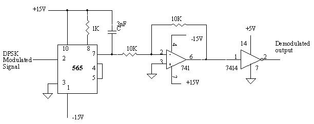
DPSK Demodulation [12,13 & 14]is done with PLL IC 565[3 4 5]. DPSK [10] signal is given as input at DPSK input terminal of PLL as shown in the figure below.
A capacitor C is connected between pin7 and power supply forms first order low pass filter with an internal resistance 3.6KW, The capacitor C should be large enough to eliminate variations in the demodulated output voltage in order to stabilize the VCO frequency. The cut-off frequency of Low pass filter is made equal to carrier frequency. The cutoff frequency of low pass filter is given by
1
fH = ———-
2pRC
R = 3.6KW, fH = 18.7KHz
The value of C designed by
1
C = ———-
2pRfH
1
C = ——————— = 2.3nF
2px3.6Kx18.7K
C selected is 3nF


hi…..what signals are given under the name W and Y???
dats a li’l confusing…
pls clarify my doubt soon..
i want information about depsk can u plz tel me about in detailed????
Truly wonderful desgin of this web page. It really is individual and compares for your posts. Don´t give up and make your individual issue!
what r flead and flag signals
why r FET’s used??..
can u plz give the detailed information of how the transmission takes place
pls send a detailed waveforms consisting of delays
i c’t understand the mean of y,w.
furla bags outlet
I have few blogs and very sporadically run out from to post .
Hi your web-site url: http://studentprojects.in/articles/electronics/analog/dpsk-modulation-and-demodulation/ seems to be
redirecting to a completely different web page when I click the home page button. You might want to
have this looked at.
What’s up, just wanted to mention, I loved this post.
It was helpful. Keep on posting!
There’s certainly a lot to find out about this issue.
I like all of the points you’ve made.