Study about PCI Bus protocol before reading this project
1.1. System Design Introduction:
The present design is of a PCI based system consisting of three Masters and six Slaves. The masters communicate with the slaves using the PCI bus. The transaction is governed by the standard PCI bus transaction protocol. Whenever a master needs to communicate with any of the slaves through the PCI bus it requests for the control of the bus to the arbiter. The arbiter grants the master control of the bus depending on the availability of the bus and also on the requesting master’s priority. Once the master is granted control of the bus it starts the transaction by keeping the address of the target slave along with the transaction command. The address thus kept is read by all the slaves. This address is decoded by each of them individually. If the address belongs to them, that particular slave acknowledges the call. This is the address phase. The address phase lasts for just one clock cycle. Once the address phase is finished the data phase begins. If none of the slaves acknowledge the masters call then the master aborts the transaction.
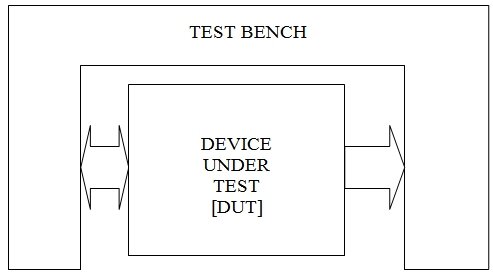
The design verification is done using the testbench. The testbench is connected to the design using channels. The testbench tells the master what transaction is to be carried out and also inspects the data sent and received at the slave end. The block diagram is as given below.

1.2. System
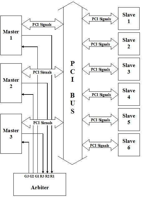
This section describes the working of the present design in brief. The block diagram of the system is as shown in below fig.
The DUT consists of Master module, Slave module, Arbiter module, Channel declaration and a top file which connects all the instances. Just one module of the master is defined and three objects are instantiated in top file. The same is being done with the slave module, just one slave module is being described and six objects are being instantiated from it in the top file.
The interconnections of all the modules are shown below. Each of the blocks is as described below.

1.2.1 Master :
In the fig5.2 Master 1, Master 2 and Master 3 are all instances of the main module Master. The master receives packets of information from the test bench. This packet contains information regarding address of the destination, command definition and data. It also tells which master is to carry out the transaction. Once the master receives and decodes this packet it begins the required transaction.
Whenever a master has to undertake any transaction it first requests the arbiter for permission to take over the bus. Once the arbiter has granted the request, the master begins the required transaction.
The transaction begins with the master by asserting FRAME#. At the same time it keeps the address of the destination along with the transaction command definition. This is called ‘Address phase’. Once the address phase is done, the master asserts IRDY# and waits for the addressed slave to asserts DEVSEL#. If DEVSEL# is not asserted until the latency time runs out, the master ends the transaction with ‘Master abort’. If DEVSEL# is asserted the ‘Data phase’ begins. The data transaction between the master and slave takes place only when both IRDY# and TRDY# are asserted. As soon as TRDY# is asserted the master places the data on the AD lines during write transaction and during read transaction it reads the data from the bus after assertion of TRDY#. All signal assertions are done during the negative clock edge and are sampled during the positive clock edge. Care should be taken to see that the signals or data on the AD lines are stable during the positive edge of the clock pulse. The master can make the target wait for the data by deasserting the IRDY# signal.
Parity of AD, C/BE and PAR are checked regularly during each phase (data/address). During write transaction the master keeps the data on the multiplexed AD lines during one clock cycle and keep its parity during next clock cycle. During a read transaction the master checks for parity during the second clock cycle of the received data. If parity is found to be odd, it asserts the PERR# during the third clock cycle. This will result in ‘Master abort’.
In some cases the slave might be ready to carry out the present transaction that the master is requesting. During such a situation the master should end the transaction and retry after some time, but with the same address and command definition. The end of the transaction is marked by deassertion of FRAME#. The FRAME# might be deasserted after the last data has been transferred or just before the last data phase. Once all the data are transferred or received IRDY# is deasserted.
1.2.2 Slave :
In fig 5.2, Slave 1 – Slave 6 are the instances derived from the module called Slave. Each slave is assigned with a unique address that is used by the master to notify which slave it wants to interact with. The address is assigned while the object of slave is instantiated.
Before a slave undertakes nay memory or i/o based transactions its configuration space should be configured. In the present design this is done by any of the masters. Rest of the transactions are done depending on the content present in the configuration space. In our design we have implemented the configuration space using a structure. Once the slave has been configured it is ready to undertake any of the transactions.
The transaction begins when the master asserts FRAME#. During the address phase all the slaves read the address placed on the AD lines. In the same clock pulse each slave compares the read address with the content stored in the base address registers present in the configuration space. If the address belongs to any particular slave it acknowledges by asserting DEVSEL# in the next clock cycle. If the slave is ready to undertake the required transaction it asserts TRDY# along with DEVSEL#. But, if the slave is not ready to undertake the required transaction it asserts STOP# instead of TRDY# telling the master to retry the same try the same transaction after some time. Once TRDY# and IRDY# are asserted the data transfer takes place. If IRDY# is not asserted then the slave has to wait until the master asserts it. The slave has to wait until the master asserts it. The slave can also make the master wait by deasserting TRDY# and asserting it only when it is ready to receive/send data.
The memory and i/o space are implemented in the monitor. The slave extracts the address of the destination location from the address that is being sent from the maser and sends it to the monitor along with the data to be stored or retrieved.
In case of blast transaction if the slave is not able to continue with any more transaction it aborts the transaction. There are three ways a slave can abort a transaction – ‘Target Abort’, ‘Target abort with data’ and ‘Target abort without data’. In ‘Target abort’, the slave needs to abort if just asserts STOP# and at the same time deasserts DEVSEL# as well as TRDY#. In ‘Master abort without data’, as soon as STOP# is asserted only TRDY# is deasserted. DEVSEL# is deasserted only clock pulse after FRAME# is deasserted. In this case no data is transmitted one the STOP# is asserted. During ‘Target abort with data’, one data phase is allowed after STOP# is asserted. After one data phase has been completed TRDY# is deasserted. The rest of the deassertion are similar to that of target abort without data.
Parity of AD, C/BE and PAR are checked regularly during each phase (data/address). During read transaction the slave keeps the data on the multiplexed AD lines during one clock cycle and keeps its parity during next clock cycle. During a write transaction the slave checks for parity during the second clock cycle of the received data. If parity is found to be odd, it asserts the PERR# during the third clock cycle. This will result in ‘Target abort’.
1.2.3 Arbiter :
Since the PCI Bus accommodates multiple masters — any of which could request the use of the bus at any time — there must be a mechanism that allocates use of bus resources in a reasonable way and resolves conflicts among multiple masters wishing to use the bus simultaneously.
The arbiter is used to grant permission to the requesting master. When more than one master is requesting, the arbiter takes in all the requests and decides which master should be granted the permission of using the bus. The arbiter selects the master depending on its priority i.e. the requesting master with the highest priority is selected first by asserting the GNT# signal. In case of multiple requests the grant is given using ‘Round Robin’ logic. The grant is given by asserting the respective GNT(G1,G2,G3) signal. Every master is connected to the arbiter by individual REQ(R) and GNT(G) signals as seen in the fig 1.2. REQ# and GNT# are unique on a per master basis allowing the arbiter to implement a bus fairness algorithm. Arbitration in PCI is “hidden” in the sense that it does not consume clock cycles.

Please send me the full project report and Code of project.